


[From Chisato Horiuchi in Tokyo]
Việc phát triển và giới thiệu các vật liệu mới cho vật liệu nền bán dẫn, trong đó silicon đã được sử dụng trong một thời gian dài, đã có nhiều tiến bộ. Trong xe điện (EV), bắt đầu với việc được Tesla của Mỹ chấp nhận, các chất bán dẫn sử dụng silicon cacbua (SiC) làm chất nền đang lần lượt được giới thiệu. Ngoài các chất bán dẫn hợp chất sử dụng SiC và gali nitride (GaN), việc nghiên cứu và phát triển kim cương và các loại tương tự cũng sẽ được tiến hành. Mặc dù giới hạn của việc thu nhỏ mạch có thể nhìn thấy được, nhưng chúng tôi mong muốn cải thiện hơn nữa hiệu suất với các vật liệu mới.
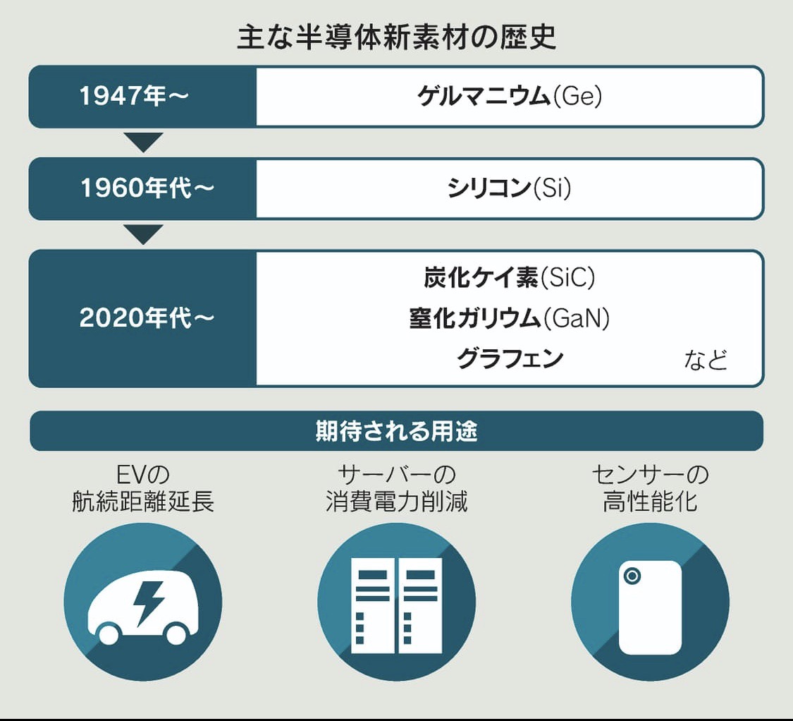
Các thiết bị điện tử như điện thoại thông minh và máy tính cá nhân sử dụng nhiều chất bán dẫn khác nhau như CPU (bộ xử lý trung tâm) và bộ nhớ, nhưng hầu hết chúng hiện được sản xuất bằng silicon làm vật liệu nền. Germanium được sử dụng một thời gian sau khi Phòng thí nghiệm Bell của Hoa Kỳ phát minh ra bóng bán dẫn vào năm 1947, nhưng kể từ những năm 1960, silicon, loại dễ kiếm và dễ gia công, mới là xu hướng chủ đạo.
Trong những năm gần đây, ưu thế tuyệt đối của nó đang sụp đổ trong các chất bán dẫn công suất cho EV. Người khởi xướng là Tesla. Công ty là một phần của EV "Model 3" hàng đầu và đã bắt đầu sử dụng chất bán dẫn sử dụng chất nền SiC lần đầu tiên trong các phương tiện sản xuất hàng loạt cho biến tần điều khiển động cơ.

SiC là một loại hợp chất cacbon và có liên kết nguyên tử với nguyên tử mạnh hơn silicon, khiến nó trở thành chất cứng thứ ba trên thế giới sau kim cương và cacbua bo. Trong khi công nghệ tiên tiến được yêu cầu để sản xuất hàng loạt, một khi nó trở thành tinh thể, các đặc tính của nó là ổn định, do đó, tổn thất điện năng tiêu thụ của chất bán dẫn có thể giảm xuống dưới một nửa.
Hiệu quả tản nhiệt cũng cao, dẫn đến biến tần bị thu nhỏ. Giáo sư Masayoshi Yamamoto của Đại học Nagoya cho biết, "Giá trị lực cản không khí của Model 3 thấp ngang ngửa với một chiếc xe thể thao. Thiết kế tinh gọn được thực hiện bằng cách giảm kích thước biến tần."
Với vai trò là người khởi xướng Tesla, động lực áp dụng xe điện đang ngày càng gia tăng. Infineon Technologies, một công ty bán dẫn lớn của Đức, đã giới thiệu một mô-đun SiC cho biến tần EV vào tháng Sáu. Takeizumi Kozu, một tập đoàn Nhật Bản cho biết: “Thời điểm lan truyền của SiC rõ ràng là sớm hơn so với dự kiến trước đây. Hyundai Motor Co., Ltd. của Hàn Quốc đã quyết định sử dụng Infineon SiC cho EV thế hệ tiếp theo của mình. Người ta nói rằng phạm vi bay có thể được mở rộng thêm 5% hoặc hơn so với silicon vì sự mất mát tiêu thụ điện năng bị triệt tiêu.
Vào tháng 6, Renault của Pháp đã hợp tác với hãng bán dẫn khổng lồ STMicroelectronics (Thụy Sĩ) để cung cấp các chất bán dẫn SiC và GaN sau năm 2026. Toyota Motor đã áp dụng SiC của Denso cho mẫu xe chạy pin nhiên liệu mới "MIRAI" được phát hành vào cuối năm 2008.
Công ty nghiên cứu France Yor dự đoán rằng thị trường bán dẫn điện sử dụng SiC sẽ mở rộng lên 4.478,2 triệu USD vào năm 2014, gấp hơn 6 lần so với 20 năm.

Application development of various new materials is progressing to follow SiC. One of the leading stocks is GaN. This technology was developed in Japan as a blue light emitting diode (LED) substrate, and if applied to a power semiconductor substrate, it can be expected to reduce power loss to about one-tenth that of silicon. Compared to SiC, it has the advantage of being able to handle high-speed operation.
Although it has already been put to practical use in some applications such as chargers, most of the products are combined with other materials such as silicon, and the original performance of the material has not been fully exhibited. A research group led by Professor Yusuke Mori of Osaka University is developing a technology for stable mass production of 6-inch diameter wafers using only GaN in collaboration with Toyoda Gosei and others.
■ "Next to silicon" development one after another
Behind the continuous research and development of new materials, there is a limit to the performance improvement of existing semiconductors. Until now, the miniaturization of circuits based on "Moore's Law", which doubles the performance of semiconductors in 18 months to 2 years, has been supported, but at present, the circuit line width is 5 nanometers (nano is one billionth of a meter). There is a view that it has been put into practical use and the physical limit is near.
Momentum for energy saving also supports development. If the performance improvement of semiconductors is delayed, EVs and data centers may consume enormous amounts of electric power. While various methods such as stacking chips are being tested, expectations are high for new materials to replace silicon, and there are a series of projects in the research and development stage.
LAB91, a spin-out from the University of Texas at Austin, is developing a technology to improve performance by stacking carbon atom sheet "graphene" on a wafer. It succeeded in the experimental stage and entered into mass production verification with a semiconductor manufacturer. It is used for camera parts of cars and smartphones, and is used for improving the performance of CMOS (Complementary Metal Oxide Semiconductor) sensors and LEDs that play the role of "eyes".
Adamand Namiki Precision Jewels (Adachi, Tokyo) and Saga University have developed a power semiconductor manufacturing technology using diamond, which is also called the "ultimate semiconductor material" because of its more stable characteristics than SiC. Theoretically, power loss can be reduced to 1 / 50,000 compared to silicon.
The problem with diamonds was to increase the size of the substrate, but we succeeded in producing the world's largest 1-inch size factory by devising the process. At the laboratory stage, we were able to produce the minimum 2 inches required for device production. However, at present, the manufacturing cost of diamond substrates is several thousand times that of silicon. How to reduce this cost is important for practical use.
Development of materials other than substrates is also progressing. ARIECA, a US spin-out from Carnegie Mellon University, has developed a material that combines a liquid metal with excellent thermal conductivity and a rubber-like stretchable material called an "elastomer." It is used as a medium for metal parts used to cool semiconductors, and has a heat dissipation effect of 50% or more compared to conventional materials.
As for semiconductors, a technology for integrating a plurality of semiconductors in one package is attracting attention as a performance improvement measure instead of miniaturization. The problem is that heat is generated when integrated at a high density, but if the company's technology is realized, a large number of circuits can be integrated in a limited volume to improve computing performance.
The Ministry of Economy, Trade and Industry announced its semiconductor strategy in June, which included support for research and development and investment in "innovative materials" such as SiC, GaN, and gallium oxide. In addition to Europe and the United States, where major power semiconductor companies are located, China is also focusing on promoting new materials. The battle for hegemony has begun toward "next to silicon" to further improve the performance of semiconductors. (Hideaki Tatsumoto, Yasu Zhang, Naoki Watanabe)


